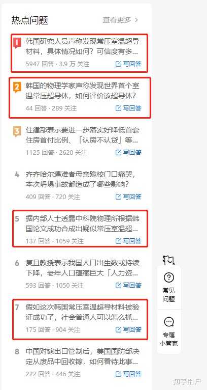
韩国的物理学家声称发现世界首个室温常压超导体,如何评价该超导体?
室温超导圣杯又被摘下了?韩国的物理学家声称,发现世界首个室温常压超导体 ——LK-99。这次能预定诺奖吗?室温常压超导,又被人突破了?这次,是韩国科学家。他们声...

- 8 个点赞 👍
继续观望吧,最快今天就会有一些实验室给出结果(以下是搬运的推文)


查看全文>>
天之骄子 - 1555 个点赞 👍
谨慎乐观,乐见其成
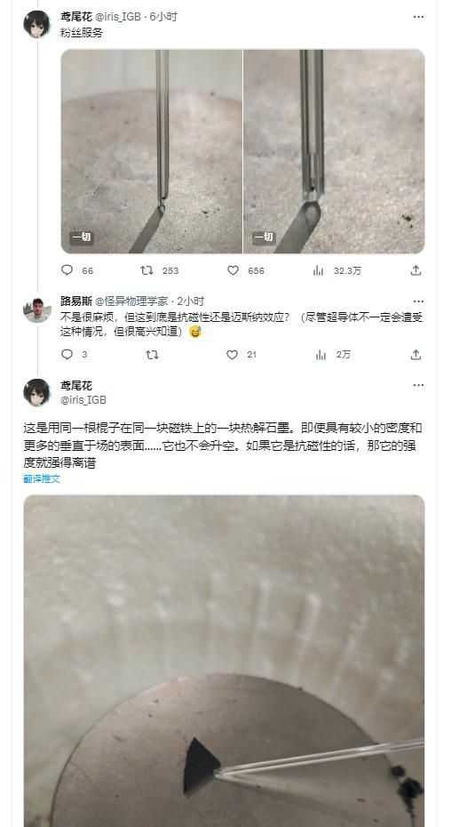
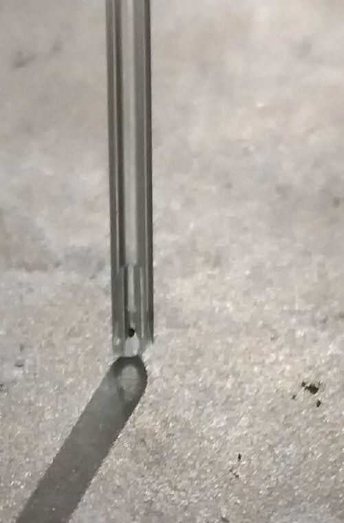
该疑似超导体说白了就是铜掺杂的铅磷灰石,用铜原子来替换其中的铅原子。由于铜的尺寸比铅小,该替换过程导致晶格畸变,引发内应力,其实是模拟了高压实验引发晶格收缩导致超导的情形。作者可能认为既然高压能通过引发晶格畸变来大幅度提高超导转变温度, 那化学方法也应该可以。这无疑是一个非常非常巧妙的思路。
进一步的理论解释,其实要追踪到二十多年前一二作者已故导师的文章,认为实现超导要做到无机原子形成一维无机高分子链。电子可以在这一维链上离域化,导致极大增强的导电性。这个理论,非常有意思,当然这里目前还是只是简单概括一下。而目前的主流理论,其实是不足以解释这个LK-99的(倘若真)。
目前主要的困境还是这个材料制备挑战性非常非常大,请不要轻信什么这个材料非常好做的传言。两个作者研究了二十多年,合成出来材料的质量还根本不够做比较可靠的物理表征,初估样品中超导相,即使存在,那么含量也很低(1%左右)。倘若能合成纯度很高,甚至单晶的样品,问题早就解决了。问题是怎么合成呢?
合成方面的主要挑战在哪里呢?在于铜掺杂的铅磷灰石这一步。这相当于要把铅磷灰石作为前驱体,再用铜敲掉一部分铅,并停留在铅的位置上。有点像斯诺克。这无疑是十分难以控制的。掺杂过程中铅磷灰石可能就先垮掉了相当一部分,毕竟高温下铜进入前驱体的过程是个扩散过程,不好控制。可想而知,目前样品中有太多各种缺陷和杂质。这种材料拿去做测试,数据一定是相当丑陋的。
这个情形有点像石墨烯当年的情况。其实回顾文献,早在Geim等人之前,就有很多人通过各种方法合成了不同品质的石墨烯。但是谁敢说自己的样品是石墨烯这种理论上不应该存在的东西呢?只有Geim通过撕胶带搞到了品质极高的样品,一举定乾坤。有了石墨烯的案例做前车之鉴,我愿意对于和我头脑里既定知识存在冲突的实验现象抱有尊敬(只要没造假)。谦虚谨慎。
现在看来,该团队在开发CVD技术做高结晶性的薄膜,我猜测还是拿铅磷灰石做成膜做前驱体,铜通过气相往里掺杂,而不是简单地烧炉子。不知道作者有没有留什么后手?诸位烧马弗炉的同行,已经落伍了。我们还是要期待进一步的结果。现在已经验证了论文作者并没有像之前Dias一样大胆造假,但是完备的超导方面的验证过程应该还会持续一段时间,甚至好几年,而且理论上的比较完备的解释很可能要等更长时间。
注:细说一下石墨烯这个“前车之鉴”
目前常见的生产石墨烯的方法,除了用胶带剥离这一种,其他的在Geim之前都报道过。很多研究人员其实在Geim之前都得到过石墨烯,例如电化学插层石墨做膨胀石墨电极材料时水面上薄薄的一层灰,但是没人那么重视。甚至直接扔掉了。但凡有个人捞起来那层灰,看看TEM,石墨烯可能就是他发现的了。另外,Geim胶带剥离石墨烯的方法很可能灵感来源于用胶带清理石墨表面脏东西的做法,这其实是处理石墨基底的常见操作。也就是说,在Geim之前,得到石墨烯的人其实有一大把。但是,大多数含有石墨烯的样品都当成垃圾扔掉了。编辑于 2023-07-28 16:25・IP 属地瑞士查看全文>>
要淡定 - 154 个点赞 👍
室温常压超导体 LK99论文机翻
注:以下全文为翻译软件机翻,如有涉及专利权等法律问题,请联系作者删除。
正文
我们有史以来第一次成功地合成了在环境压力下工作的室温超导体(T c ≥ 400 K,127 o C),并具有改进的铅-磷灰石(LK-99)结构。 用临界温度(Tc)、零电阻率、临界电流(Ic)、临界磁场(Hc)和迈斯纳效应证明了LK-99的超导性。 LK-99的超导性源于轻微体积收缩(0.48%)的微小结构失真,而不是温度和压力等外部因素。 收缩是由Pb(2)-磷酸盐绝缘网络中Pb2+(2)离子的Cu 2+取代引起的,并产生应力。 它同时将圆柱柱传输到Pb(1),导致圆柱柱界面失真,从而在界面中产生超导量子阱(SQW)。 热容结果表明,新模型适用于解释LK-99的超导性。 LK-99的独特结构允许在界面中保持微小的扭曲结构,这是LK-99在室温和环境压力下保持和表现出超导性的最重要因素。
For the first time in the world, we succeeded in synthesizing the room-temperature superconductor (T c ≥ 400 K, 127 o C) working at ambient pressure with a modified lead-apatite (LK-99) structure. The superconductivity of LK-99 is proved with the Critical temperature (Tc ), Zero-resistivity, Critical current (Ic ), Critical magnetic field (Hc ), and the Meissner effect. The superconductivity of LK-99 originates from minute structural distortion by a slight volume shrinkage (0.48 %), not by external factors such as temperature and pressure. The shrinkage is caused by Cu 2+ substitution of Pb2+ (2) ions in the insulating network of Pb(2)-phosphate and it generates the stress. It concurrently transfers to Pb(1) of the cylindrical column resulting in distortion of the cylindrical column interface, which creates superconducting quantum wells (SQWs) in the interface. The heat capacity results indicated that the new model is suitable for explaining the superconductivity of LK-99. The unique structure of LK-99 that allows the minute distorted structure to be maintained in the interfaces is the most important factor that LK-99 maintains and exhibits superconductivity at room temperatures and ambient pressure.
介绍
自发现第一个超导体(1)以来,通过其实验清晰度或/和理论视角(4-8),世界各地已经进行了许多寻找新室温超导体的努力(2,3)。 最近开发含硫化氢(9)和钇超氢化物(10)的室温超导体的成功受到全世界的极大关注,这是与高频氢声子模式的强电子-声子耦合理论所预期的(11,12)。 然而,由于压力极高,很难在日常生活中将其应用于实际应用设备,并且正在做出更多努力来克服高压问题(13)。
我们有史以来第一次报告了用化学方法合成室温和环境压力超导体以解决温度和压力问题的成功情况。 我们命名了第一个室温和环境压力超导体LK-99。 通过临界温度(Tc)、零电阻率、临界电流(Ic)、临界磁场(Hc)和迈斯纳效应(14、15)证明了LK-99的超导性。 收集并详细分析了几个数据,以找出LK-99超导性的难题:X射线衍射(XRD)、X射线光电子光谱(XPS)、电子顺磁共振光谱(EPR)、热容和超导量子干扰器件(SQUID)数据。 从今以后,我们将报告和讨论我们的新发现,包括与LK-99超导率相关的超导量子阱。
Since the discovery of the first superconductor(1), many efforts to search for new room-temperature superconductors have been carried out worldwide(2, 3) through their experimental clarity or/and theoretical perspectives(4-8). The recent success of developing room-temperature superconductors with hydrogen sulfide(9) and yttrium super-hydride(10) has great attention worldwide, which is expected by strong electron-phonon coupling theory with high-frequency hydrogen phonon modes(11, 12). However, it is difficult to apply them to actual application devices in daily life because of the tremendously high pressure, and more efforts are being made to overcome the high-pressure problem(13).
For the first time in the world, we report the success in synthesizing a room-temperature and ambient-pressure superconductor with a chemical approach to solve the temperature and pressure problem. We named the first room temperature and ambient pressure superconductor LK-99. The superconductivity of LK-99 proved with the Critical temperature (Tc ), Zero-resistivity, Critical current (Ic ), Critical magnetic field (Hc ), and Meissner effect(14, 15). Several data were collected and analyzed in detail to figure out the puzzle of superconductivity of LK-99: X-ray diffraction (XRD), X-ray photoelectron spectroscopy (XPS), Electron Paramagnetic Resonance Spectroscopy (EPR), Heat Capacity, and Superconducting quantum interference device (SQUID) data. Henceforth in this paper, we will report and discuss our new findings including superconducting quantum wells associated with the superconductivity of LK-99.

图1.(a)测量电压与 在不同温度下施加电流,(b)薄膜零电阻率,(c)测量电压与 各种外部磁场(Oe)下的应用电流,(d)10 Oe磁场的场冷却和零场冷却的直流磁化,(e)临界电流与 临界温度,(f)临界电流与 临界磁场。
图1(a)显示了不同温度(298 K~398K)下的测量电压与施加电流,图1(a)的测量是在10-3 Torr的真空中,直流(DC)极性变化3的真空中每增加20K温度。 在各种散装样品中,测量了10-6至10-9Ω·cm的特异性电阻。 此外,通过热蒸汽沉积工艺在精密玻璃板上制备了LK-99薄膜(UNIVAC,韩国)。 图1(b)显示了LK-99薄膜的零电阻率,它满足了国际标准(16,17)作为新型超导体的零电阻率。 根据国际电工委员会的标准(16),超导率有两个等效标准(17):1μV/cm或0.1μV/cm的电场标准和10-11Ω·cm的电阻率标准。 如图1(b)所示,在施加电流增加和减少期间,测量的电压在0.1μV/cm范围内得到。 此外,电阻率按10-10~10-11Ω·cm的顺序计算。 随着晶界的减少,薄膜的残余电阻降低(18)。 图1(c)显示了施加电流的外部磁场(H)依赖性。 即使高达400K,零场冷却和10 Oe的现场冷却的直流磁化值在图1(d)中仍然为负值。 这些结果表明,超导相在10 Oe下仍然存在,最高可达400K。 此外,即使在图1(e)和(f)中400K和3000 Oe或更多时,临界电流值也不是零(7 mA)。 因此,我们判断LK-99的临界温度超过400K。 此外,由于LK-99具有图2所示的多晶形态,散装样品的不均匀电阻率可以解释为晶间边界、粒际涡流、多晶超导相的自由涡流(18-20)。 还观察到超导体-正常金属-超导体(21、22)或粒际耦合超导体(23)阻尼连接的约瑟夫森样现象(补充材料中的图S1(a))以及粒内或粒内网络的热电效应(补充材料中的图S1(b))。
Figure 1(a) shows the measured voltage vs. applied current at various temperatures (298 K ~ 398K), the measurement for Figure 1(a) was performed with direct current (DC) polarity change by each 20 K increment of temperature in the vacuum of 10 -3 Torr. In various bulk samples, specific resistance was measured in the range of 10 -6 to 10 -9 Ω·cm. Also, a thin film of LK-99 was fabricated on the precision glass plate by a thermal vapor deposition process (UNIVAC, Korea). Figure 1(b) shows the Zero-resistivity of the thin film of LK-99, which satisfied the zero-resistivity of international standards(16, 17) as a new superconductor. According to the International Electrotechnical Commission standards(16), there are two equivalent criteria(17) for superconductivity: the electric field criterion with 1 µV/cm or 0.1 µV/cm and resistivity criterion with 10 -11 Ω·cm. As shown in Figure 1(b), the measured voltage was obtained in the range of 0.1 µV/cm during the applied current increasing and decreasing. Also, the resistivity was calculated in the order of 10 -10 ~ 10 -11 Ω·cm. As the grain boundary is decreased, the residual resistance of the thin film decreased(18). Figure1(c) shows the external magnetic field (H) dependence of applied current. Even up to 400 K, the DC magnetization value of Zero field cooling and Field cooling with 10 Oe was still negative in Figure 1(d). These results indicate that the superconducting phase still exists under 10 Oe up to 400 K. Additionally, the critical current value was not yet zero (7 mA) even at 400 K and 3000 Oe or more in Figure 1(e) and (f). Therefore, we judge that the critical temperature of LK-99 is over 400 K. Moreover, since LK-99 has a polycrystalline morphology shown in Figure 2, the non-uniform resistivity of the bulk samples can be explained as inter-grain boundaries, intergranular vortex flow, free vortex flow(18-20) of polycrystalline superconducting phase. The Josephson-like phenomenon (Figure S1(a) in supplementary materials) for the under-damped junction of superconductor-normal metal-superconductor(21, 22) or Intergrain coupled superconductors(23) and the thermoelectric effect(24-26) of the inter- or intra-grain network(Figure S1(b) in supplementary materials) were also observed.

图2。 LK-99的XRD结果与COD匹配,原始XRD数据仅被Kα2条纹,无需任何其他处理。
图2显示了LK-99与QualX2.0软件(27)匹配的结果,并通过使用VESTA软件(28)的模拟数据证明,该软件使用晶体学开放数据库(COD)执行搜索匹配操作(27)。 它表明LK-99是多晶的。 主要峰值与铅-磷灰石(AP)结构非常匹配,也很少显示Cu2 S杂质。 原始铅-脂肪矿的晶体系统是六边形的(P63 /m,176),细胞参数为a=9.865 Å和c=7.431 Å。 然而,与参数为a=9.843 Å和c=7.428 Å的铅磷灰石相比,LK-99略有收缩。 LK-99的体积减少为0.48%。 人类早就知道,物质的性质源于其结构。 然而,到目前为止,超导性和材料结构变化之间的相关性几乎没有得到适当澄清。 事实上,到目前为止发现的影响超导体超导产生的两个主要因素是温度和压力(29、30)。 温度和压力都会影响它的体积。 在低温或高压下体积下降所产生的应力似乎会导致微小的应变或失真。 虽然很难观察到超导材料的微小结构变化,但这种结构变化似乎带来了超导性。
Figure 2 shows the results of LK-99 matched with the QualX2.0 software(27) and proved by simulated data using VESTA software(28), which uses Crystallography Open Database (COD) to perform the search-match operation(27). It shows that LK-99 is polycrystalline. The main peaks were well matched with the lead-apatite (AP) structure, and few Cu2 S impurities also shown. The crystal system of the original lead-apatite is hexagonal (P63 /m, 176) with the cell parameters a=9.865 Å and c=7.431 Å . However, LK-99 shows a slight shrinkage compared to the LeadApatite with parameters of a=9.843 Å and c=7.428 Å . The volume reduction of LK-99 is 0.48 %.
Humankind has long learned that the properties of matter stem from its structure. However, so far, the correlation between superconductivity and the structural change of material has hardly been properly clarified. In fact, the two main factors affecting the generation of superconductivity of superconductors discovered so far are temperature and pressure(29, 30). And both temperature and pressure affect its volume. It seems that the stress generated by the decrease in volume under the low temperature or high pressure causes a minute strain or distortion. Although it is difficult to observe the minute structural changes in superconducting materials, this structural change seems to bring the superconductivity of it.
显示外部因素(压力和温度)和内部因素(掺氧)造成的超导性的代表性例子是基于CuO的超导材料。 根据掺氧含量,CuO的结构从四边形结构转变为正交结构。 此外,在高压条件下观察到较高的Tc(29)。 在基于CuO的超导体中,可以认为c轴以及a轴和b轴变化量不一致产生的应力影响中间CuO层,导致结构失真和超导性,因为c轴的变化似乎对温度和压力的变化最敏感。 其他例子是我们认为由精细物理应力引起的失真或应变引起的超导性外观。 当绝缘子顶部的FeSe单层堆叠时,最高T c达到65 K(31),甚至高达109 K(32)。 然而,随着图层堆栈的增加(33-35),T c降至10K。 在Bi2 Sr2 Cu2 O8+δ上的CuO单层薄膜中,Zhong等人确定了两个不同且空间分离的间隙:U样间隙和V样间隙(36)。 2019年,Choi等人证明了3D应变对板条系统(37)的T c的影响,BaFe2 As 2系统在2013年也显示了应变诱导的超导性(38)。 2008年,Gozar等人报告了金属和绝缘氧化铜之间的高温界面超导性(39)。 层越薄,应力诱导效应越大,应变越大,这似乎是超导过渡温度越高。 因此,我们认为,温度和压力引起的应力会带来微小的结构失真和应变,从而产生超导的电子状态。
Representative examples showing the superconductivity due to the external factors (pressure and temperature) and the internal factors (oxygen doping) are CuO-based superconducting materials. The structure of CuO changes from the tetragonal structure to the orthogonal structure depending on the oxygen doping contents. In addition, the higher T c is observed under the high pressure condition(29). In the CuO based superconductors, it may be thought that the stress generated by the inconsistency of the amount of change in the c-axis and a and b-axis affects the intermediate CuO layer, causing structural distortion, and superconductivity because the changes in the c-axis seems to be the most sensitive to changes in temperature and pressure. And other examples are what we think of as the appearance of superconductivity caused by distortion or strain caused by fine physical stress. When the FeSe monolayer on the top of the insulator is stacked, the highest T c achieves up to 65 K(31) and even up to 109 K(32). However, the T c lowers to 10 K as layer stacks increases (33-35). In the case of CuO monolayer films on Bi2 Sr2 Cu2 O8+δ , Zhong et al. identified two distinct and spatially separated gaps: U-like gap and V-like gap(36). In 2019, Choi et al. proved the effect of 3D strain for T c in the cuprate system(37), and BaFe2 As 2 system also showed strain-induced superconductivity(38) in 2013. In 2008, Gozar et al. reported hightemperature interface superconductivity between metallic and insulating copper oxides(39). The thinner the layer, the greater the stress-inducing effect, the greater the strain, which seems to be the higher the superconducting transition temperature. Therefore, we argue that the stress caused by temperature and pressure brings a minute structural distortion and strain, which create an electronic state for superconductivity.
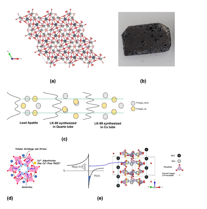

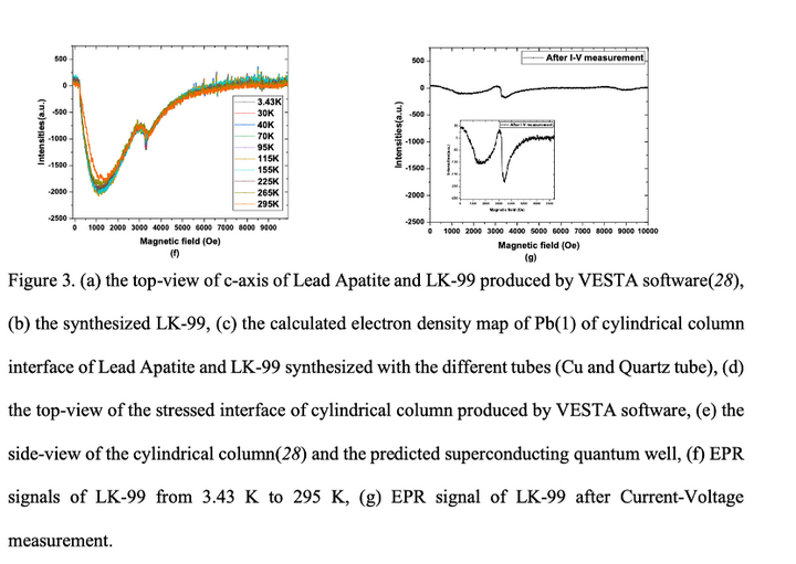

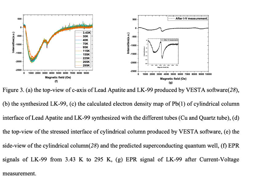
图3.(a)VESTA软件生产的铅磷灰石和LK-99的c轴顶视图(28),(b)合成的LK-99,(c)磷灰石铅圆柱界面Pb(1)和用不同管(Cu和石英管)合成的LK-99的计算电子密度图,(d)VESTA软件生产的圆柱应力界面的顶视图,(e)圆柱柱的侧视图(28)和预测的超导量子阱,(f)LK-99从3.43 K到295 K的EPR信号,(g)电流电压测量后LK-99的EPR信号。
LK-99是灰黑色,如图3(b)所示。 它是与典型超导体颜色相同的超导体。 铅-脂肪矿(40),Pb10(PO4)6 O系统,是一种象牙色粉末和绝缘体。 LK-99具有图3(a)所示的三维网络结构和由绝缘四面体PO 4网络结构包围的圆柱形柱。 间隔为6.541Å的圆柱由不对称多面体六个Pb(1)-O n分量组成,由两个形状相反的三角形组成,如图3(e)中圆柱的侧视图所示。 多面体四Pb(2)是LK-99绝缘PO 4网络结构的组件。 LK-99的改性铅磷灰石预计为Pb10- x Cux(PO4)6 O,x=0.9~1.0,其中四个Pb(2)离子中的一个大约已被铅-脂肪(41)多面体Pb(2)位点的Cu(II)离子取代。 在LK-99中,铜的比例是根据XPS的原子百分比数据确定的,并由具有热容结果和化学式Pb10-x Cux(PO4)6 O,x=0.9~1.0的Debye热容模型确认。 它与之前公布的研究结果(41)非常一致。 这种在LK-99中替换Cu 2+离子导致体积减少0.48%,因为Cu 2+离子(87 pm)小于Pb 2+离子(133 pm)。 应力发生在网络部分,然后影响超导性的外观。
LK-99 is a gray-black color, as shown in Figure 3(b). It is the superconductor with the same color as typical superconductors. The system of lead-apatite(40), Pb10 (PO4 )6 O, is an ivory-colored powder and an insulator. The LK-99 has a three-dimensional network structure shown in figure 3(a) and a cylindrical column surrounded by an insulating tetrahedral PO 4 network structure. And the cylindrical columns arranged at intervals of 6.541 Å are composed of asymmetric polyhedral six Pb(1)-O n components consisting of two oppositely shaped triangles as shown in the side-view of the cylindrical column in Figure 3(e). The polyhedral four Pb(2) are components of insulating PO 4 network structures of LK-99. The modified lead-apatite of LK-99 is expected to be Pb10- x Cux (PO4 )6 O, x=0.9~1.0, in which one of the four Pb(2) ions approximately has been replaced by Cu(II) ion at the polyhedral Pb(2) sites of the lead-apatite(41). In LK-99, the ratio of copper was determined based on the atomic % data of XPS and confirmed by the Debye heat capacity model with heat capacity result and chemical formula Pb10-x Cux (PO4 )6 O, x=0.9~1.0. And it is well consistent with previous published research result(41). This replacement of Cu 2+ ions in LK-99 resulted in a volume reduction of 0.48 % because Cu 2+ ions (87 pm) are smaller than Pb 2+ ions (133 pm). The stress was occurred in the network portion and then affected the appearance of superconductivity.
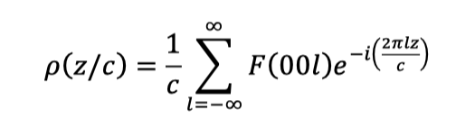
通过对XRD和XPS数据进行更精确的分析,它揭示了体积减少的压力最终受到的影响。 为了确定Pb(1)位置的变化,通过计算结构因子的傅里叶变换,沿一个晶体轴进行了一维电子密度计算(42)。 根据XRD数据的(00l)反射强度,使用以下方程计算了沿z方向ρ(c)电子密度。
As a result of more precise analysis of XRD and XPS data, it reveals where the stress from volume reduction was finally affected. For the purpose of determining the variation of Pb(1) positions, One-dimensional electron density calculation(42) along one crystallographic axis via the Fourier transform of the calculated structure factor was used. The electron density was calculated along the z-direction, ρ(c), based on the (00l) reflection intensities of XRD data using the following equation.


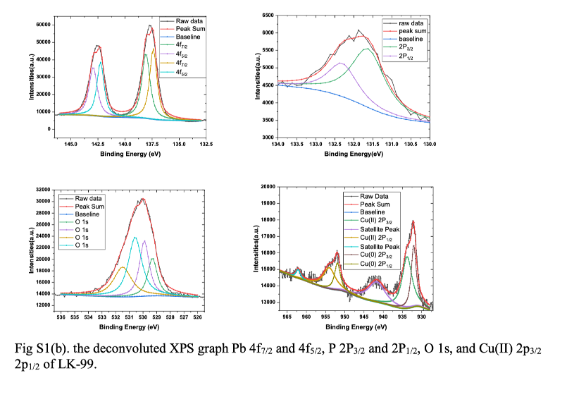
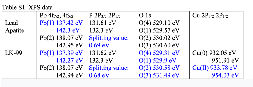
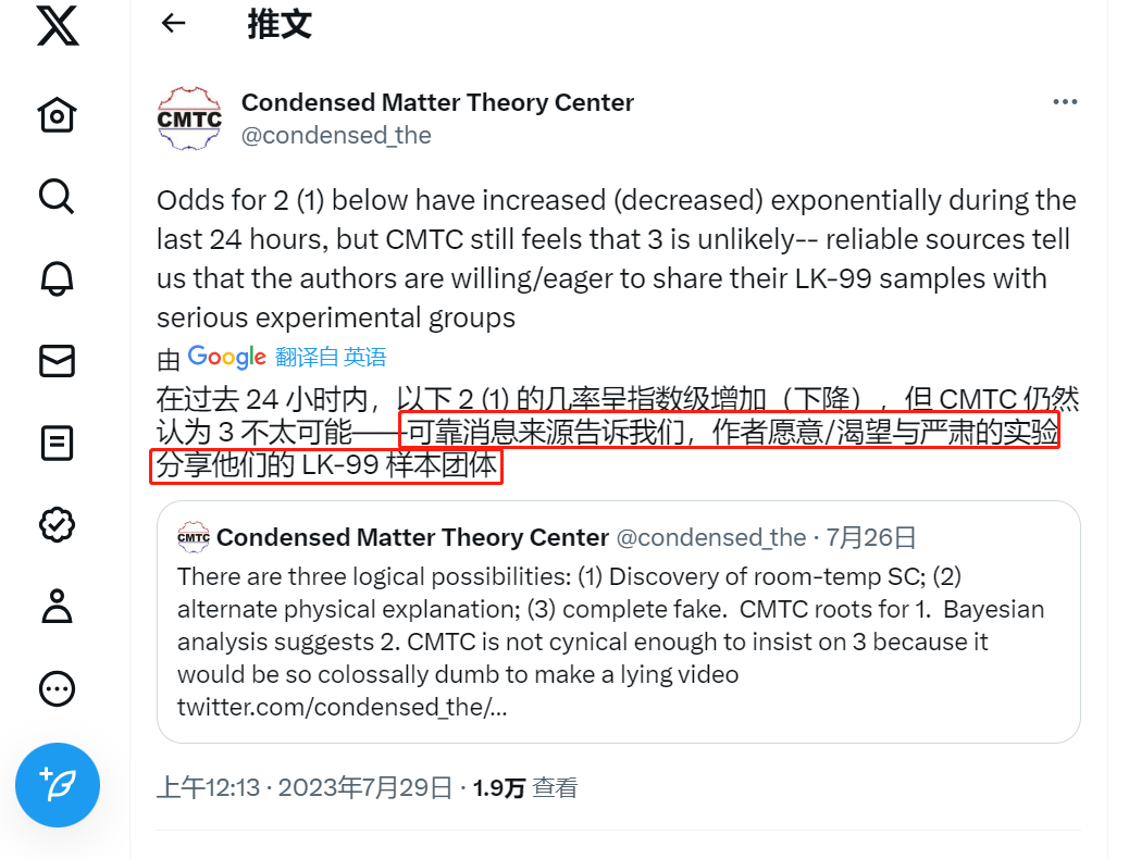
其中l、F(00l)、c和z分别是(00l)衍射峰的阶、结构因子、c轴的单位细胞参数和沿z轴的原子坐标。 由于LK-99具有六边形结构,根据图2中XRD数据的(00l)和(h00)反射强度,将上述方程应用于沿z方向(c轴)和x方向(a轴)以及ρ(c)和ρ(a)的Pb(1)电子密度计算。 因此,通过在图3(c)中向内或向外替换Cu 2+,构成圆柱柱的Pb(1)在a轴平面上的位置略有偏移。 在圆柱Pb(1)的重复三角形结构中,一层Pb(1)之间的距离从原始3.03340Å增加到2.61815Å,下一层的距离增加到5.23476Å。 然而,LK-99的Pb(1)三角形层之间穿过c轴的距离(3.7140Å)与铅-脂肪岩(3.7153Å)几乎保持不变。 根据XPS数据的分析结果,Pb(2)和磷的结合能(B.E.)保持不变。 虽然2p 3/2和2p1/2之间的四面体磷分裂值非常小,从0.68 eV增加到0.69 eV,所有氧B.E.分别增加了0.21 eV、0.33 eV、0.56 eV和0.89 eV。 此外,Pb(1)的B.E.值略有下降0.03 eV。 从上述结果中可以看出,体积减少是由铜2+离子的替换引起的,体积减少引起的应力导致Pb(1)的位置变化和Pb(1)附近氧原子之间的结合能变化。 图3(f)显示了LK-99的EPR信号。 它与异质结量子阱相同,如Si/SiGe(43),干燥状态的天然DNA(44)和掺杂Mg2+的α-Fe2 O3(45)。 EPR信号被解释为量子阱二维电子气体(2-DEG)的回旋加速器共振信号,这也证实了LK-99的Pb(1)和磷酸盐界面中量子阱的形成。 此外,如图3(f)所示,替换的Cu 2+离子出现在3000 Oe的EPR信号中。 据报道,GaAs/AlGaAs(46)和DNA(47)的2-DEG系统的超导性为0.3K和1K。 具有界面结构的超导体,如2-DEG系统的异质结,如LaAlO3 /SrTiO3(48-50),已被证明具有超导性。 因此,经证实,超导量子阱(SQW)是通过结构畸变和应变在磷(1)和磷酸盐氧之间产生的。 预测的SQW如图3(e)所示。 LK-99的超导性与SQW密切相关。 2002年,Koji等人已经报告了如图3(f)所示的类似的EPR信号和RuSr2 GdCu2 O8系统(51)的超导性。 然而,他们没有将EPR信号解释为SQW,并将其与超导性的外观联系起来。
Where l, F(00l), c and z are the order of the (00l) diffraction peak, the structure factor, the unit cell parameter of the c-axis, and the atomic coordinate along the z-axis, respectively. Since LK-99 has a hexagonal structure, the above equation was applied for the electron density calculation of Pb(1) along the z-direction (c-axis) and x-direction (a-axis), and ρ(c) and ρ(a), based on the (00l) and (h00) reflection intensities of XRD data in Figure 2. As the result, the position of Pb(1) constituting the cylindrical column is slightly shifted in the a-axis plane from the original position by the substitution of Cu 2+ inward or outward in Figure 3(c). In the repeated triangular structure of Pb(1) of the cylindrical column, the distance between Pb(1) in one layer is decreased to 2.61815 Å , and the next layer is increased to 5.23476 Å from the original distance of 3.03340 Å . However, the distance (3.7140Å ) through the c-axis between the triangular layers of Pb(1) of LK-99 remains almost unchanged from lead-apatite (3.7153Å ). According to the analyzed results of XPS data, the binding energies (B.E.) of Pb(2) and Phosphorus were unchanged. Although, the tetrahedral Phosphorus splitting value between 2p 3/2 and 2p1/2 very slightly increased from 0.68 eV to 0.69 eV, and all oxygens B.E. are quite a bit increased by 0.21 eV, 0.33 eV, 0.56 eV, 0.89 eV, respectively. Also, the B.E. value of Pb(1) is slightly decreased by 0.03 eV. From the results described above, it can be seen that the volume reduction was caused by the replacement of Cu 2+ ions, and the stress caused by the volume reduction caused the position change of Pb(1) and the binding energy change between oxygen atoms adjacent to Pb(1). Figure 3(f) shows the EPR signal of LK-99. It is the same as the heterojunction quantum well such as Si/SiGe(43), natural DNA(44) in a dry state, and α-Fe2 O3 (45) doped with Mg2+ . The EPR signals were interpreted as a cyclotron resonance signal of 2-dimensional electron gas (2-DEG) of quantum well, which also confirmed the creation of quantum wells in the interface between Pb(1) and Phosphate of LK-99. In addition, the substituted Cu 2+ ions were appeared at 3000 Oe in EPR signals as shown in Figure 3(f). The superconductivity with the 2-DEG system of GaAs/AlGaAs(46) and DNA(47) was reported at 0.3 K and 1 K. The superconductor having interface structure like a heterojunction of the 2-DEG system such as LaAlO3 /SrTiO3 (48-50) has been shown the superconductivity. Hence, it is confirmed that the superconducting quantum well (SQW) was generated between Pb(1) and Oxygens of Phosphate by structural distortion and strain. The predicted SQW was illustrated in Figure 3(e). The superconductivity of LK-99 is deeply related to SQW. In 2002, Koji et al. already reported the similar EPR signals as shown in Figure 3(f) and the superconductivity with RuSr2 GdCu2 O8 system(51). However, they did not interpret the EPR signals as SQW and to associate it with the appearance of superconductivity.
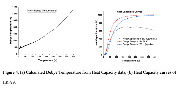

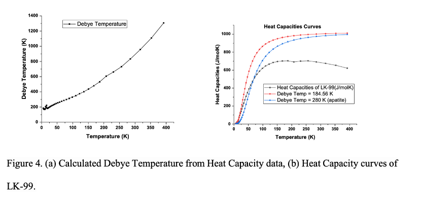
图4.(a)从热容数据计算的擦除温度,(b)LK-99的热容曲线。
使用物理性质测量系统(PPMS,DinaCool-9,Quantum Design,USA)测量LK-99的热容从5K到400K,并通过以下Debye热容方程,根据Pb10-x Cux(PO4)6 O公式(x=1)的热容数据计算了Debye温度;
The heat capacity of LK-99 was measured from 5 K to 400 K using Physical Property Measurement System (PPMS, DinaCool-9, Quantum Design, USA), and Debye temperature was calculated based on the heat capacity data using Pb10-x Cux (PO4 )6 O formula (x = 1) through the following Debye heat capacity equation;
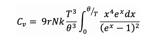

其中C v是热容,r是每个分子的原子数量,N是分子数,k是玻尔兹曼常数。 图4显示,LK-99的德拜温度不断从大约184K变化到1300K。 因此,T c无法用电子声子预测模型计算。 蓝线曲线(德拜温度=280 K)是典型磷灰石的计算热容,因为典型磷灰石的德拜温度为280 K。 红线曲线是根据LK-99低温(5K)下的Debye温度(184.56 K)计算的热容结果。 在传统超导体的情况下,电子声子模型对此进行了相对很好的解释。 在电子声子模型中,预测T c的最有影响力的参数之一是德拜温度(52)。 LK-99的热容曲线(黑线曲线)不遵循Debye模型,因为正常振动模式受到LK-99网络部分Cu 2+离子替换的限制。 这一结果还证实了LK-99的结构因Cu 2+离子的替换而失真。 根据LK-99所示的EPR实验结果,超导性的表达可以用SQW的形成来解释。 还有一篇论文用量子阱模型(36)解释了超导性。 然而,他们没有显示像我们这样的EPR信号。 图3(d)是电流电压测量后在样品(LK-99)上测量的EPR信号。 与不施加电流的信号(图3(f))相比,总体信号强度下降,回旋加速器共振的信号强度在图3(g)中相对降低。 此外,对于基于CuO的超导体,大吸收EPR信号在非常低的温度和低于1000 Oe的外部磁场(53,54)下出现,我们还观察到YBCO和Bi2212。 1000 Oe外部磁场以下的信号可以解释为超导电子的信号(53,54)。
where C v is heat capacity, r is the number of atoms per molecule, N is the number of molecules, and k is the Boltzmann constant. Figure 4 shows that the Debye temperature of LK-99 is constantly changing from about 184 K to 1300 K. Thus, T c cannot be calculated with the electron-phonon prediction models. The blue line curve (Debye temperature = 280 K) is the calculated heat capacity of the typical apatite because the Debye temperature of the typical apatite is 280 K. The red line curve is the calculated heat capacity results based on Debye temperature (184.56 K) at a low temperature (5 K) of LK-99. In the case of conventional superconductors, it is relatively well explained by the electron-phonon model. And in the electron-phonon model, one of the most influential parameters of predicting T c is Debye temperature(52). The heat capacity curve (black line curve) of LK-99 does not follow the Debye models, since the normal vibrational mode is limited by Cu 2+ ions replacement in the network part of the LK-99. This result also confirms that LK-99 has a structure distorted by the substitution of Cu 2+ ions. In terms of the EPR experimental results shown in LK-99, the expression of superconductivity can be explained by the formation of SQWs. There is also a paper explaining superconductivity with the quantum well model(36). However, they did not show EPR signals like ours. Figure 3(d) is the EPR signal measured on the sample (LK-99) after Current-Voltage measurement. Compared to the signal in which no current is applied (Figure 3(f)), the overall signal intensities decreased, and the signal intensity of cyclotron resonance was relatively decreased in Figure 3(g). Additionally, in case of CuO based superconductors, the large absorption EPR signal appeared at a very low temperature and below 1000 Oe external magnetic field(53, 54), and we also observed with YBCO and Bi2212. The signal below 1000 Oe external magnetic field can be interpreted as a signal by superconducting electrons(53, 54).
Josephson在超导体之间安装了一个薄绝缘体,并发现了电流流过的隧道。 超导体之间发生了隧道(55)。 同样,如果电子通过在SQW之间隧道移动,电阻自然为零。 SQW之间的隧道可能是可能的,因为SQW预计将在LK-99中以3.7Å~6.5Å的间隔形成。 根据Kim的论文(52),他使用1250 K的Debye温度计算室温超导体,Ashcroft(56)在1968年提到了氢化物。 即使在这种情况下,他也认为电子-电子相互作用比电子-声子相互作用具有更高的温度超导性。 在LK-99系统中,施加的电流似乎通过隧道过程通过圆柱柱的相关SQW传输,并与所有SQW一起以三维连贯传输。 关于LK-99的额外实验结果和讨论将立即发表在下一篇论文中,包括一个有趣的可控悬浮现象以及磁性和超导共存、理论计算等。 LK-99对许多研究人员来说将是一种有吸引力的物质,可以解决与超导性相关的各种令人困惑的难题,如配对过程和与磁性共存等。
Josephson installed a thin insulator between superconductors and discovered tunneling through which current flows. Tunneling occurred between the superconductors(55). Likewise, if electrons are moved by tunneling between SQWs, the resistance will naturally be zero. Tunneling between SQWs is likely to be possible, as SQWs are expected to be formed at 3.7 Å ~ 6.5 Å intervals in LK-99. According to Kim’s paper(52), he used 1250 K Debye temperature for his calculation of room-temperature superconductor, which is mentioned for hydride in 1968 by Ashcroft(56). Even in that case, he argued that the electron-electron interaction contributes to the higher temperature superconductivity than the electron-phonon interaction. In LK-99 system, the applied current seems to be transported through the correlated SQWs of the cylindrical column via the tunneling process and coherently transported in 3-dimension with all SQWs together. The additional experimental results and discussions on LK-99 will be published immediately in the next paper, including an interesting controllable levitation phenomenon and the coexistence of magnetism and superconductivity, theoretical calculation, etc. LK-99 will be an attractive substance for many researchers that can solve various confusing puzzles such as the pairing process and coexistence with magnetism, etc., related to superconductivity.
因此,为什么LK-99在室温和环境压力下表现出超导性? 这是因为由于LK-99的结构唯一性,Pb(2) 2+离子的Cu 2+替换产生的应力没有缓解,同时适当地转移到圆柱的界面。 换句话说,LK-99圆柱界面中的Pb(1)原子占据了结构有限的空间。 这些原子完全受到铜2+离子产生的应力和应变的影响。 因此,在室温和环境压力下,可以通过适当的失真(57)在界面中产生SQW,而无需松弛。 从这个角度来看,在CuO和Fe基超导体系统中,温度和压力导致体积收缩引起的应力得到了缓解和消失,因为由于结构自由度,松弛过程不能受到限制。 因此,它们需要适当的温度或压力来限制结构自由度并实现SQW生成。 LK-99是研究室温超导难题非常有用的材料。 所有证据和解释都表明,LK-99是第一个室温和环境压力超导体。 LK-99具有多种应用的可能性,如磁铁、电机、电缆、悬浮系统、电源电缆、量子计算机量子比特、THz天线等。 我们相信,我们的新发展将是一个全新的历史事件,为人类开启一个新时代.
Consequently, why does LK-99 exhibit superconductivity at room temperature and ambient pressure? This is because the stress generated by the Cu 2+ replacement of Pb(2) 2+ ion was not relieved due to the structural uniqueness of LK-99 and at the same time was appropriately transferred to the interface of the cylindrical column. In other words, the Pb(1) atoms in the cylindrical column interface of LK-99 occupy a structurally limited space. These atoms are entirely affected by the stress and strain generated by Cu 2+ ions. Therefore, SQWs can be generated in the interface by an appropriate amount of distortion(57) at room temperature and ambient pressure without a relaxation. From this point of view, the stress due to volume contraction by temperature and pressure is relieved and disappeared in CuO- and Fe-based superconductor systems because the relaxation process cannot be limited due to the structural freedom. Therefore, they need an appropriate temperature or pressure to limit the structural freedom and to achieve the SQW generation. The LK-99 is a very useful material for the study of superconductivity puzzles at room temperature. All evidence and explanation lead that LK-99 is the first room-temperature and ambient-pressure superconductor. The LK-99 has many possibilities for various applications such as magnet, motor, cable, levitation train, power cable, qubit for a quantum computer, THz Antennas, etc. We believe that our new development will be a brand-new historical event that opens a new era for humankind.
补充材料
样品合成与制备
样品合成和制备 对于LK-99的样品合成,使用了一般固态反应。 Lanarkite和Cu3 P在带有杵的玛瑙砂浆中均匀混合,摩尔比为1:1。 将样品放入反应管中,在10-5 Torr的真空下密封,并在925°C下反应10小时。 反应后,可重现获得深灰色的锭,然后制成薄立方体的形状进行电测量。 在其他分析中,它被粉碎并用作粉末的形式。 用于上述固态反应的试剂是PbO(JUNSEI,GR)、PbSO 4(KANTO,GR),Cu(DAEJUNG,EP)和P(JUNSEI,EP)。
Sample Synthesis and Preparation
For the sample synthesis of the LK-99, the general solid-state reaction was used. Lanarkite and Cu3 P were uniformly mixed in a molar ratio of 1:1 in an agate mortar with a pestle. The sample was put into a reaction tube, sealed under the vacuum of 10 -5 Torr and reacted at 925°C for 10 hr. After the reaction, a dark gray ingot was obtained reproducibly and then made into the shape of thin cuboids for electrical measurements. For other analyses, it was pulverized and used as the form of powder. The reagents used for the above solid- state reaction was PbO (JUNSEI, GR), PbSO 4 (KANTO, GR), Cu (DAEJUNG, EP), and P (JUNSEI, EP).
1)lanarkite的制备,Pb2SO5
PbO和PbSO 4粉末在带有杵的玛瑙砂浆中均匀混合,摩尔比为1:1。 然后,在样品转移到氧化铝坩埚中后,它在725°C的炉子中反应24小时。 反应完成后,获得了白色样品。 它被砂浆粉碎了。
1) Preparation for lanarkite, Pb2 SO5
PbO and PbSO 4 powders were uniformly mixed in a molar ratio of 1:1 in an agate mortar with a pestle. And then, after the sample was transferred to an alumina crucible, it was reacted at 725 °C for 24 hour in a furnace. After completion of the reaction, white sample was obtained. It was pulverized with the mortar.
2)制备磷化铜,Cu3 P
在每个成分比例中混合了铜和磷粉。 样品被转移到石英管中。 管子在10-5 Torr的真空下密封,并在550°C的炉子中反应48小时。 从管子中取出后,获得并粉碎了深灰色的锭子。
2) Preparation for copper phosphide, Cu3 P
Cu and P powders were mixed in each composition ratio. And the sample was transferred in a quartz tube. The tube was sealed under the vacuum of 10 -5 Torr and reacted at 550 °C for 48 hour in a furnace. After taken out from the tube, a dark gray ingot was obtained and pulverized.
电气性能测量设置
4点探针测量使用4个四个pogo测试探头(YoungJinSa,Inc.,韩国)相互绝缘,并排列成一条相同距离(1.2毫米)的线。 Keithley 228A和Keithley 182分别用作电压/电流源和敏感数字电压表。 为了准确的温度控制和测量,我们开发并使用了带有隔热铝安装板和卤素灯的自设计的加热装置作为加热源。 使用LabView软件的自行开发软件也用于测量。 所有测量仪器都与GPIB接口设备相连。 使用Keithley 2000在样品表面使用FLUKE 80BKDMM K型热电偶探头进行了温度测量。
Set-up for electrical properties measurement
4-point probe measurement was performed with 4 four pogo test probes (YoungJinSa, Inc., Korea) insulated from each other and arrayed in one line with the same distance (1.2mm). The Keithley 228A and Keithley 182 were used as voltage/current source and sensitive digital voltmeter, respectively. For accurate temperature control and measurement, we developed and used the self-designed heating device with a thermally insulated aluminum mounting plate and halogen lamp, as a heating source. The Self-developed software, using LabView software, was also used for the measurement. All measuring instruments were linked with GPIB interface devices. Temperature measurement was carried out with Keithley 2000 with FLUKE 80BKDMM K-type thermocouple probe on the sample’s surface.
XRD数据的收集
在韩国大学绿色制造技术研究所绿色制造研究中心与Rigaku(日本SmartLab)收集的XRD数据XRD数据。
Collection of XRD data
XRD data collected with Rigaku (SmartLab, Japan) at Institute of Green Manufacturing Technology Green Manufacturing Research Center of Korea University.
用SQUID测量磁性(MPMS)
磁化测量使用直流模式进行,扫描长度为30毫米,每次测量扫描10次,扫描时间为10秒,使用超导量子干扰装置(韩国KAIST研究促进分析中心的MPMS3-Evercool)。 零场冷却在没有外部磁场的情况下从400K加工到200K,然后用10 Oe磁场将温度从200K提高到400K。 最后,样品在10 Oe磁场下从400K冷却到200K。 45.814毫克样本用于此测量。
Measurement of Magnetic Properties with SQUID (MPMS)
Magnetization measurement is performed with dc mode, 30 mm scan length, 10 scans per measurement, scan time 10s by using Superconducting Quantum Interference Device (SQUID) (MPMS3-Evercool of KAIST Analysis Center for Research Advancement, Korea). Zero fieldcooling is processed from 400 K to 200 K without external magnetic field and then the temperature is increased from 200 K to 400 K with 10 Oe magnetic field. Finally, the sample is cooling down from 400 K to 200 K with 10 Oe magnetic field. The 45.814 mg sample is used for this measurement.
电子顺磁共振光谱测量
EPR光谱使用JESFA200 ESR X波段光谱仪在3.45 K至295 K的温度范围内进行(日本Jeol)。 入射微波功率为0.9980 mW,接收器增加100和扫描时间(1分钟)。 调制磁场在100 KHz下为10 G,扫荡外部磁场为-100 ~ 9,900 Oe或0 Oe ~ 10,000 Oe。 LK-99样品设置在5毫米石英管中(Wilmad LabGlass,美国),在I-V测量之前,LK-99密封真空(5 x 10 -5 torr),在I-V测量后,LK-99样品没有密封真空。 然后将密封的石英管装入配备液氦低温器系统的气缸腔(美国高级研究系统)。
Measurement of Electron Paramagnetic Resonance Spectroscopy
EPR Spectroscopy is performed over the temperature range from 3.45 K to 295 K using a JESFA200 ESR X-band spectrometer (Jeol, Japan). The incident microwave power is 0.9980 mW,the receiver gains 100 and the sweep time (1 min). The modulated magnetic field is 10 G at 100 KHz and the swept external magnetic field is -100 ~ 9,900 Oe or 0 Oe ~ 10,000 Oe. The LK-99 sample is set in a 5 mm quartz tube (Wilmad LabGlass, USA), sealed vacuum (5 x 10 -5 torr) for LK-99 before I-V measurement, not sealed vacuum for LK-99 sample after I-V measurement. And then the sealed quartz tube was loaded into a cylinder cavity equipped with a liquid helium cryostat system (Advanced Research Systems, USA).
用PPMS测量热容量
在下一代半导体收敛技术研究所(DGIST,韩国)使用物理性质测量系统(PPMS)(DynaCool-9,量子设计,美国)收集了5K至400K和65.26毫克LK-99的热容量数据。 原始数据使用Cu2 S散装和纳米片的热容参考进行了校准,纳米片作为杂质包含在少量中。
Measurement of Heat Capacity by PPMS
The heat capacity data were collected from 5 K to 400 K with 65.26 mg of LK-99 using by Physical Property Measurement System (PPMS) (DynaCool-9, Quantum Design, USA) in Institute of Next-generation Semiconductor convergence Technology (DGIST, Korea). And the raw data was calibrated with heat capacity references of Cu2 S bulk and nanosheet, which is included in a small amount as an impurity.
铅-磷灰石和LK-99的X射线光电子光谱(XPS)研究
XPS数据收集自韩国大学绿色制造技术研究所绿色制造研究中心ULVAC-PHI(日本X-TOOL)。 Pb、P、O和Cu的XPS数据使用XPSPEAK 4.1软件进行解卷曲。 使用雪莉背景函数校正背景,并使用洛伦兹(80%)-高斯(20%)和函数进行拟合。
X-ray Photoelectron Spectroscopy (XPS) Study on the lead-apatite and LK-99
XPS data collected from ULVAC-PHI (X-TOOL, Japan), Institute of Green Manufacturing Technology Green Manufacturing Research Center of Korea University. The XPS data of the Pb, P, O and Cu are deconvoluted using XPSPEAK 4.1 software. The background is corrected using the Shirley background function and the Lorentzian (80%)-Gaussian (20%) sum function is used for fitting.


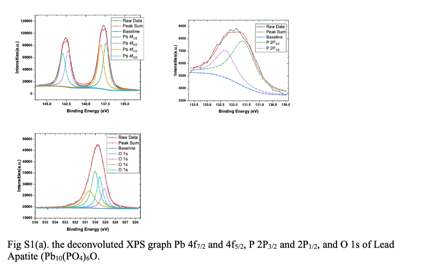
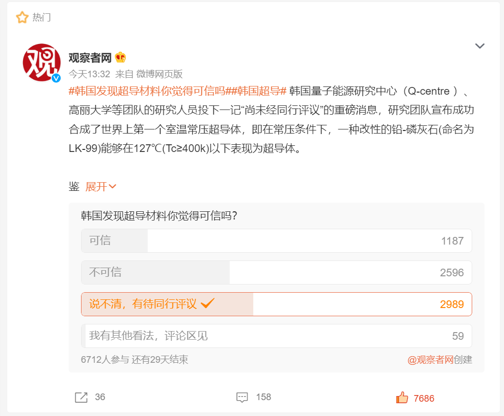
在Cu的XPS结果中,结合能(B.E.) 932.05 eV,951.91 eV来自Cu(0)原子,这是反应物Cu3 P的残基。只有933.78 eV,954.03 eV来自LK-99基质的替代Cu(II)离子,其余是Cu(II)离子的卫星峰。 原子取代量是使用相对原子灵敏度计算的。 结果约为Cu/Pb=0.9/10。
In the XPS results of Cu, Binding Energy (B.E.) 932.05 eV, 951.91 eV is come from Cu(0) atom, which is residue of reactant Cu3 P. the only 933.78 eV, 954.03 eV are from the substituted Cu(II) ion of LK-99 matrix, the rest are satellite peaks of Cu(II) ions. And the amount of atomic substitution is calculated using the relative atomic sensitivity. The result is about Cu/Pb=0.9/10.

看看表S1,Pb(1)和Pb(2)之间Pb(1)的B.E.略有变化。 四个Pb(2)离子由磷灰石的网络结构组成,六个Pb(1)离子由正文中的圆柱组成。 四种不同类型的氧气与Pb(1)和Pb(2)结合,并形成像图S3一样的多面体结构。
Looking at the table S1, there is a little change in B.E. of Pb(1) among Pb(1) and Pb(2). The four Pb(2) ions is composed of the network structure of apatite, and six Pb(1) ions is composed of the cylindrical column in main text. And four different types of oxygen are bonded to Pb(1) and Pb(2) and made a polyhedral structure like a Figure S3.
 编辑于 2023-07-28 09:27・IP 属地黑龙江
查看全文>>
注册账号2 - 105 个点赞 👍
原来的内容被全部删除,但是问题又冲上了热搜,说明原问题不是被“和谐”,而是被平台删帖。
我认为知乎上的热门回答应当被视作一种公共财产,受到法律保护。而不是平台想删就删。
发布于 2023-07-28 12:07・IP 属地黑龙江查看全文>>
JFK的头 - 98 个点赞 👍
查看全文>>
安德罗勃夫 - 46 个点赞 👍
(本回答持续更新)
2023.7.29 9:34
Andrew McCalip继续上线直播验证,距离开锅还剩2个钟半时间。
2023.7.29 8:36
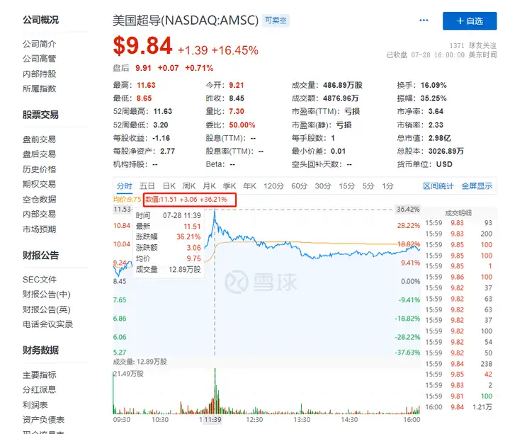
欧美市场反应:美国超导概念一度暴涨到36.21%

2023.7.29 8:25
马里兰大学凝聚态理论中心(CMTC)透露:韩国研究团队愿意拿LK-99样品给别的实验组做测试


2023.7.29 8:01
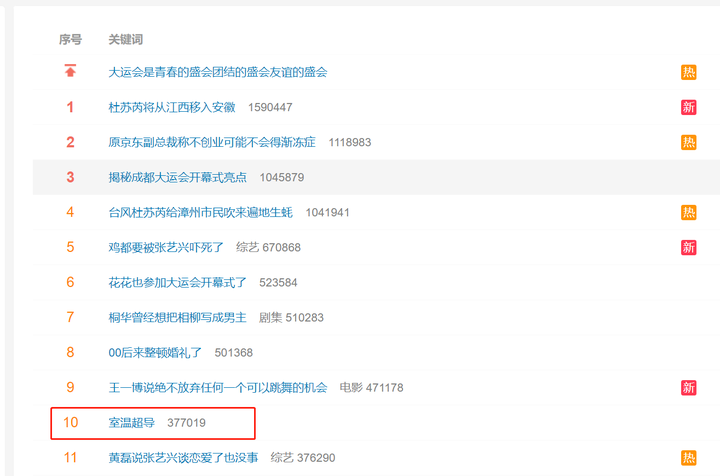
目前超导话题,在微博热搜第10位,知乎平台浏览量破亿。


19:13
微博网友对常温超导事件的看法:


18:54
知乎平台上,超导事件热度未减,真热搜需要移步创作中心的“热点问题”:

18:42
推上这个大壮在直播烧铅块:


直播网站:
编辑于 2023-07-29 10:13・IP 属地广东真诚赞赏,手留余香还没有人赞赏,快来当第一个赞赏的人吧!查看全文>>
Salye - 30 个点赞 👍
这个常压室温超导材料没用实用性。
常温超导有什么用?想了半天没想出来,长途输送电力性质的输电线路这块肯定想都不要想,省下来的那点电的收益根本不够买超导材料的零头,运行一百年也回收不了当年的线路架设投资。
在仪器、设备上用?也不行,先不说超导材料又脆又硬、不能反复弯折,现有的电路如果都用超导材料,这些电路反而会变得又粗、又重,根本就没法布设在电路板上,并且使用寿命、可靠性会由于太容易断开,变得反而不如金属材料。
虽然如此,这依然是人类科学的一大进步,但真的没有用。
陈平:电磁炮,磁悬浮交通这些磁场类应用 都会减少体积和维护成本
答陈平:抱歉,这些领域都用不上。以电磁炮左右二侧的滑道为例,金属氧化物的热胀冷缩特性,让电磁炮左右二侧的滑道必须是拼接结构,因为电磁炮左右二侧的滑道长度一般都超过十米,而拼接的接缝就是无解的有电阻,还有瞬间的高温会烧蚀电磁炮左右二侧的滑道,对于常温超导材料,我相信这种烧蚀是可以破坏超导性的。还有电磁炮发射时巨大的震动,会很容易震碎电磁炮左右二侧的滑道。综上,现在的这个方向上的所有常温超导材料都没有实用性。
铁轨由于热胀冷缩,需要在二个铁轨之间留下缝隙,常温超导材料的导电电路也这样做?金属氧化物的材料不能焊接,不能用螺栓压接,因为可能被压碎,张紧的金属氧化物材料在机械震动下会彻底碎掉,电磁弹射线圈甚至发电机线圈都可以在几小时之内彻底震碎常温超导材料制成的线圈。
如果发现的常温超导材料是金属,那立即就会被大规模的应用开来,一个新的工业革命会立即爆发。现在的这种金属氧化物,企业想用也用不上,不能焊接,不能螺纹连接,不能铆接,二个石头之间甚至可以说不能连接,那还怎么大规模的推广应用?!
虽然如此,这依然是人类科学的一大进步!这一点无可否认。
编辑于 2023-07-29 09:44・IP 属地北京真诚赞赏,手留余香还没有人赞赏,快来当第一个赞赏的人吧!查看全文>>
零距离常数 - 29 个点赞 👍
只能说,如果是假的,甚至是数据造假,我愿称他们为“世界上获得感最低的一群造假者”。
因为,实验的复刻,最快的已经有了初步结果,大面积实验室结论,可能明天就会有集中发布。从论文的发布,到对实验的验证,造假的话,“获得感”周期,低到不足一周时间。
付出的代价,则是Young-Wan Kwon和Hyun-Tak Kim的整个学术生涯,前者是高丽大学教授,赌上的不仅是自己,而且还有高丽大学的学术声誉。
高丽大学(Korea University)与首尔大学(Seoul National University)和延世大学(Yonsei University)并称为韩国大学的一片天(S.K.Y.)。
后者,则是威廉玛丽学院的教授,一位万引作者。
(最有意思的是,整个事件里,被认为最有可能通过造假受益的Sukbae Lee和Jihoon Kim,反倒是最淡定的两个人。
而获得收益最小,承担风险最大的Young-Wan Kwon和Hyun-Tak Kim,前者抢发论文,现在正在高丽大学做相关报告,后者则针锋相对,第一个接受采访,直言Young-Wan Kwon上传的第一篇论文未经自己允许,并直接将Young-Wan Kwon移除作者名单,可谓互不相让。)
Sukbae Lee和Jihoon Kim从1999年第一次发现并以两个人的名字命名LK-99,如今已经走过了23年时间,他们两个人从未站到前台,即使关注如现在,仿佛一切的喧嚣与热闹,从来都不属于他们。
发布于 2023-07-28 21:30・IP 属地北京真诚赞赏,手留余香还没有人赞赏,快来当第一个赞赏的人吧!查看全文>>
来去的加菲 - 12 个点赞 👍
如果是真的,诺贝尔奖未来几年估计都得是超导材料相关,地球ol上线工业4.0版本应对玩家流失。
如果是假的,恭喜这位占卜家途径的研究者完成了世界范围的愚弄,建议保送序列0。

 发布于 2023-07-28 22:53・IP 属地河南
查看全文>>
舟舟 - 3 个点赞 👍
查看全文>>
联邦Terra分部 - 2 个点赞 👍
北京时间2:46美国加州最新消息:复现成功!复现出来的材料纯度不高,但是!该材料确实为常压常温超导体!mit材料实验室也已经验证成功了,第四次工业革命真的开始了!遗憾的是,作为普通人,能做的只有等待,诶,希望能活得久一点吧!人类终将走向星辰大海!全网第一成功复现链接放出https://b23.tv/b49fgVN
发布于 2023-07-29 10:16・IP 属地山东查看全文>>
登临意 - 2 个点赞 👍

个人拙见 根据韩国那个论文是让铜原子替换然后靠内应力形成长城般的超导链 最难的是形成那么长的链条 已知石墨烯是单层结构原子 宏观可见 能不能用类似失腊法的效果 其他材料浇筑石墨烯然后把石墨烯想法去除 灌注其他元素 这或者不成了一组组超导链了吗[思考]
编辑于 2023-07-29 20:36・IP 属地山东查看全文>>
智库长 - 2 个点赞 👍
查看全文>>
DCAFT - 1 个点赞 👍
占个坑,如果真的电阻极小,想让他们测一下耐用性(时间),还有是否有类似于银的电迁移(这是为什么用金线去bonding)。还有这种物质的力学特性如何,能否弯曲,弯曲后能否负载射频信号,与传统的导体是否在负载射频信号方面有类似的表现即信号是否只在表面传输。做个阻抗谱出来,扫个频。耐多少温度能依旧保持超导形态,有没有记忆性。
这些问题算是应用端需要考虑的部分问题,如果事实证明这种超导体构建方法论可行的话,几年时间类似的文章肯定是络绎不绝。如果能避开一些局限,那么电学的书籍很多都要改写,半导体工艺的布线问题也能得到很大的优化,我国的EDA没准能实现弯道超车,虽然我们工艺方面可能暂时上不去。
编辑于 2023-07-29 08:41・IP 属地江苏查看全文>>
Grant - 1 个点赞 👍
查看全文>>
丸子 - 1 个点赞 👍
本来是要在一周之后才能得出终极结论,但现在复现实验出现一个颇有些劲爆的消息:多国权威机构或物理学科学家们实现了初步样品的完成,复现实验结果为——成功。
这意味着,人类可能会见证继前一、二、三次工业革命之后的第四次工业革命的兆头。
紧接着,为了验证这一不可思议的消息,各大硬核型的相关领域精英们纷纷传递着本群的交流信息,似乎都在指向‘大有希望’的可能性。
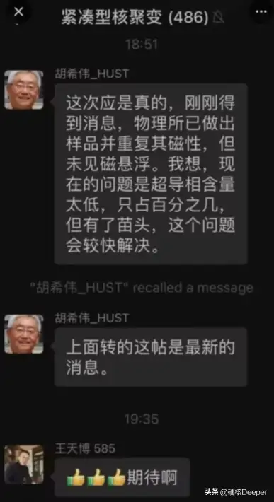
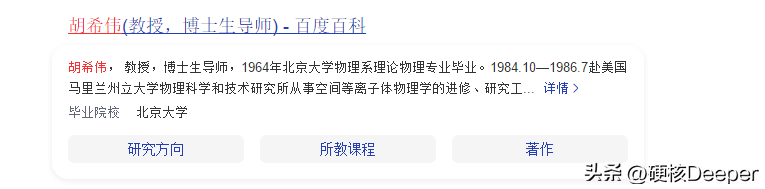
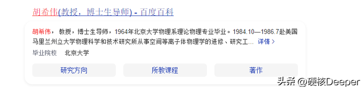
就像这个聊天截图中的‘胡希伟’,竟是从美国进修回来的物理专业的大牛,这就更加增进了信源的可信度。

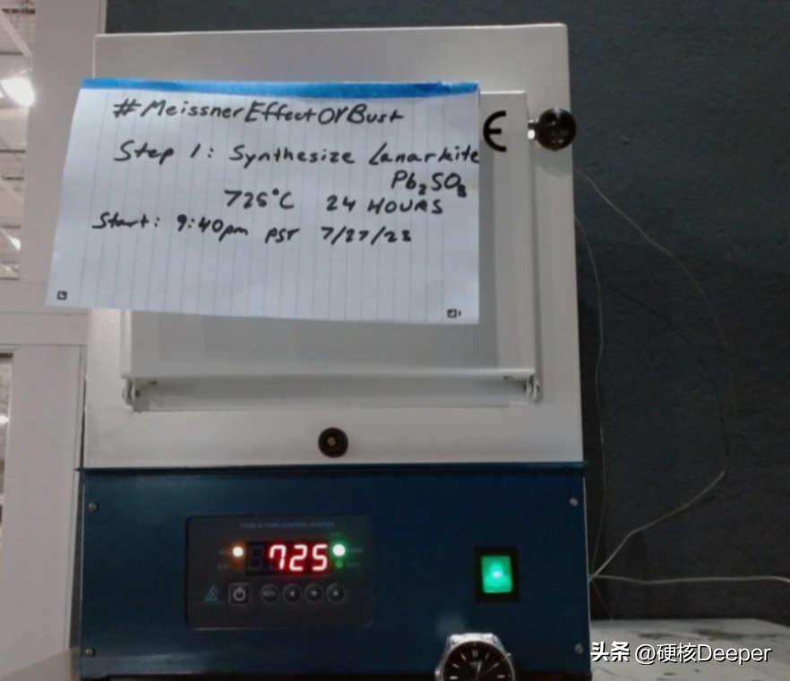
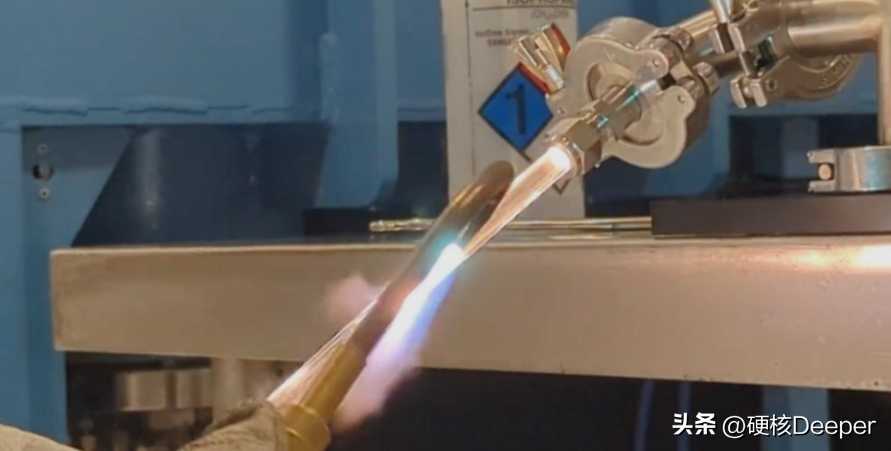
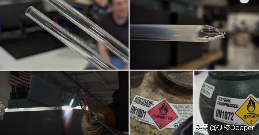
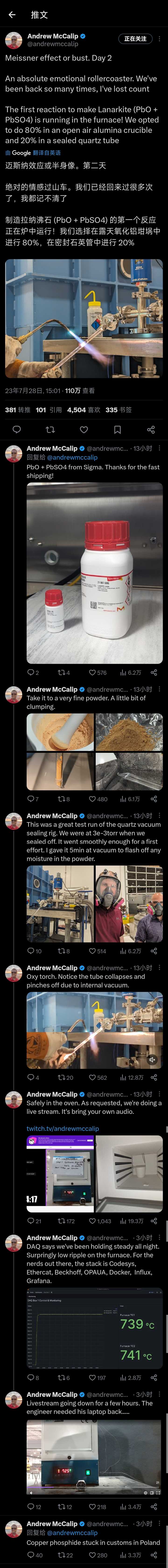
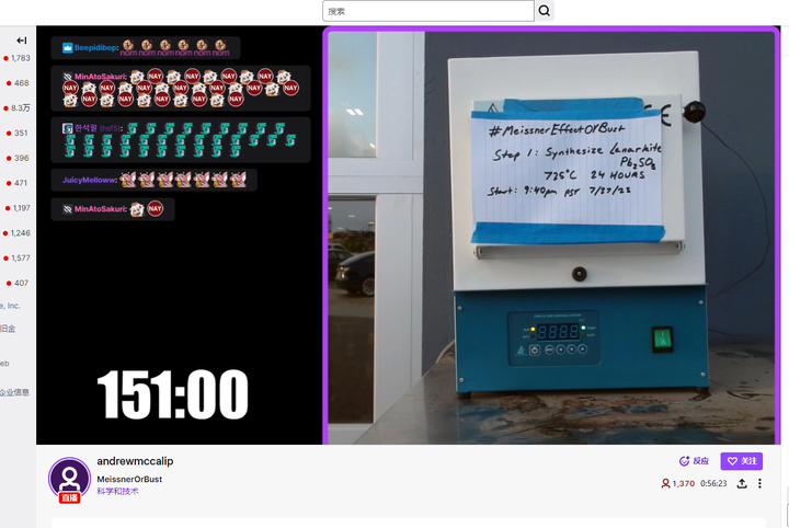
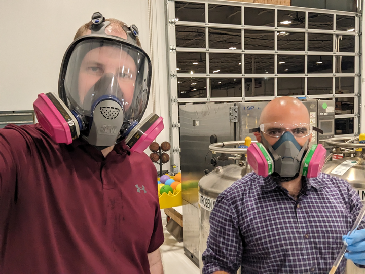
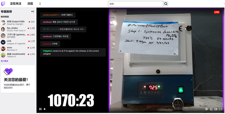
黄铅矿合成 PbO + Pb(SO4) ,需用时24小时,相关的硬核主播其实都是各大研究员和研究小组做复现实验的过程呈现,
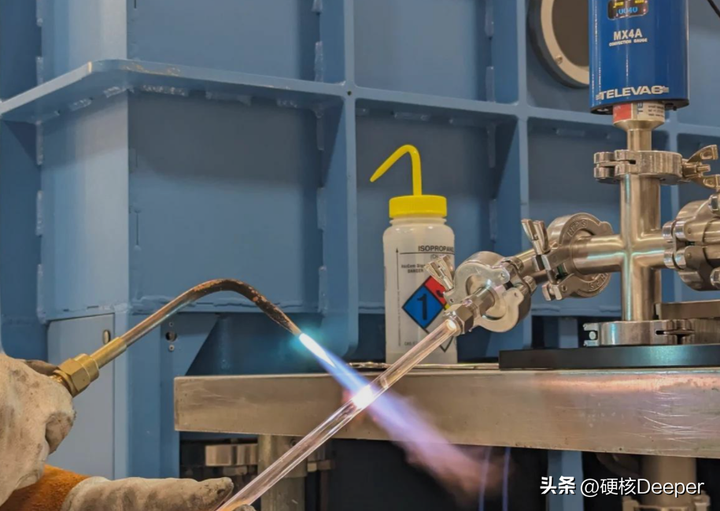

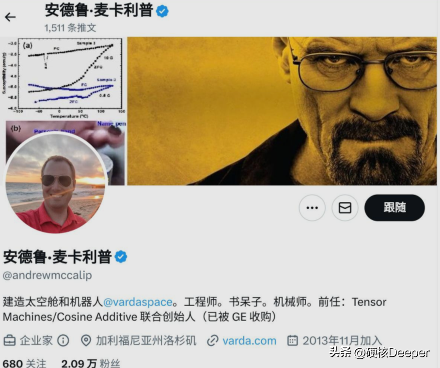
我们回来了很多次,我已经记不清了制造拉纳克石(PbO + PbSO4)第一个反应是在熔炉中运行——安德鲁正在实验
这位安德鲁是绝对的技术宅,因为他本身的职业就很硬核,工程师,机械师,面对韩国这次的‘偶然性发现’的相对以往更加简单的合成材料公式,他得心应手,不在话下。
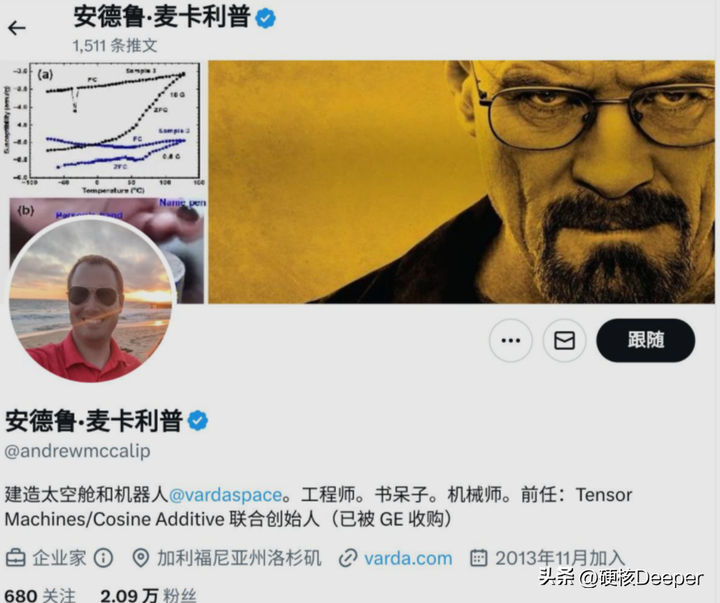

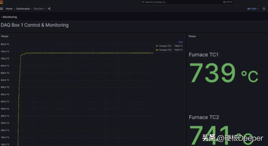
安德鲁说:“我们整个晚上都保持稳定。炉子上的波动出奇地低。对于那些书呆子来说,技术栈是 Codesys、Ethercat、Beckhoff、OPUAA、Docker、Influx、Grafana。”


在看到温度稳定时,他已经有点激动了:

他还有一个同样有兴趣陪他一起做实验的‘同伴’——托马斯。
他们抓住了焊件旋转工作台定位器,并将其变成了管道夹具,他说到:“用踏板控制来翻转管子真是太好了,我们是业余爱好者,但这感觉像是可行的。”

如科学们做重大实验的科学记录步骤一样,他们正在做着每个步骤的记录,结尾还不忘吐槽一句相关材料可能要大卖了,有人可能会因此而发财,但前提得是韩国的发现彻底成真。
1000c 退火炉 - 已到位
氧乙酰炬 - 已到位
石英安瓿 - 已到位
高真空泵 - 已到位
玻璃加工技能 - 已到位
红磷 - 未到位
Sigma Aldrich 明天会想知道为什么他们有成千上万的人订购氧化硫酸铅而购买红磷是需要DEA许可证的,所以目前很多‘同步复现实验室’的原材料购买和运输反而也成了一道不大不小的障碍,争分夺秒的过程中,谁都不想只是因为材料难到手而放弃或让实验结论出现得太晚。
这就是他们购买的材料,还不忘记录一下,表示自己要坚决做下去,毕竟这可能会让人类见证历史。


质疑至此,全世界都不太关心实验本身所涉及的‘杂质’的难题了,因为一旦初步得出可靠的结论,验证了常压室温超导物质的存在,那么人类想什么办法都会做出纯的出来。
尤其是这种世界已达成共识的“非常廉价”的制造方法,有一定可能大规模制造的常温超导,它的前景就可以比拟任何一个现有行业的。

氧气火炬。请注意,由于内部真空,管子会塌陷并被夹断。
而随着现在全球经济萎靡的现状,现目前确实是太多人迫切的希望能出现一场新工业革命改变现在的生活状态,而这些人不是几个,甚至是几亿,几十亿人,但凡有相关认知和常识的人都能意识到这东西成真到底意味着什么。
我相信,大家、也包括我在内,都不希望它最终只是一个闹剧,相反,都在等待最终的结果。总而言之,科学的发现,必须要用科学的方式才会令人信服,最终结论未实锤之前,我们保持对未来的期待,在这个过程中,所有人都应该是愉悦的。


真空密封石英管,实验室已经获得了相当不错的管端。这将远低于 1e-5torr。
有人说,中科院这次的回复是不是太慢了?我反而认为,若是中科院回复的越久,可能恰恰说明这事很大,再加上这次是可立刻进行复现实验的大发现,那么大家或许都已在实验的路上了,想想,确实令人期待。
最后,告诉大家一个直观的事情,这次促成全球同步实验的原因是LK-99可容易复现,但比较耗时间,所以保持期待,静等最终结果出来。
发布于 2023-07-30 19:20・IP 属地广东真诚赞赏,手留余香还没有人赞赏,快来当第一个赞赏的人吧!查看全文>>
不負歲月年華 - 0 个点赞 👍
查看全文>>
一剑 - 0 个点赞 👍
查看全文>>
凌晨 - 0 个点赞 👍
查看全文>>
無心飛翔 - 0 个点赞 👍
查看全文>>
捷径 - 0 个点赞 👍
第一次工业革命,乾嘉时期,英法横行的时代
第二次工业革命,中国进入半殖民地半封建,美国崛起
第三次工业革命,二战后的百废待兴
现在,假设室温超导体是真的——那么拥有世界上最完备工业体系的国家,拥有最庞大受教育人口的国家,拥有基建狂魔称号的国家,可以全速发动这台工业机器了!
以前中国被迫错过发展的红利,这一次,终于赶上时代的超光速飞船了……
发布于 2023-07-29 06:07・IP 属地江苏查看全文>>
雾雨魔理沙 - 0 个点赞 👍
拭目以待吧,成功就是新工业革命,信息革命还未结束,可喜可贺。
新科学革命导致的社会进步更加明显,新科学革命在中国诞生,加油
https://www.mysmth.net/nForum/#!article/TheoPhys/47599?p=10
相对论存在两个漏洞,谁能驳倒本民科文德奎,全网直播吃屎!闵可夫斯基时刻坐标存在漏洞,光速不变原理存在实验漏洞。
为让大众简单理解相对论存在两个漏洞,出此下策,话丑理端,请来批吧!发现相对论漏洞,这是中国人的骄傲,各位吃瓜群众可以搬小凳子了。
1、国际原子时是不是时间体系核心?不是就让中科院废除国际原子时,中科院宣布后,然后本民科直播吃屎!
2、相对论时空坐标有没有国际原子时位置?公认理论闵可夫斯基时空坐标有国际原子时位置,本民科直播吃屎!
3、让中科院宣布物理现象对于物理理论不重要,毫无意义,本民科直播吃屎!
4、一束光通过匀速封闭运动空间,光通过封闭空间内外运动速度变化没有实验、分析,如果科学界有实验分析,任何结论都可以,找出来,本民科直播吃屎!
相对论存在两个漏洞(新两朵乌云):一、国际原子时在天文、物理、航空航天等中,处于核心位置,但在物理时空坐标中没有国际原子时的位置;二、一束光通过匀速封闭运动空间,光通过封闭空间内外运动速度变化没有实验、分析。
此漏洞需要与斐索实验数据、迈克尔逊实验数据、sagnac效应数据、王汝涌广义sagnac效应等等实验结合实验分析,相关论文链接在本链接一楼附件:https://www.newsmth.net/nForum/#!article/TheoPhys/47159
封闭空间比如高铁能带动内部空气、蝴蝶、雾气共同运动 ,没有人分析是否能带动光共同运动;地球能带动一定范围周围空气、云彩、飞机共同运动,没有人分析是否能带动光共同运动,而且带动一定范围光共同运动,也会导致0结果,参考迈克尔逊实验1887年原文。
相对论闵可夫斯基时间时空坐标四个变量(x,y,z,L=ct)其中 x∈(+ ∞,0,- ∞),y∈(+ ∞,0,- ∞),z∈(+ ∞,0,- ∞),L=ct∈[a,b],此时间坐标与空间坐标不对应,会导致时间维度扭曲(0表达坐标原点,与教科书不同)。
将国际原子时T纳入时间、空间坐标后,变量为(x,y,z,T),T∈(+ ∞,0,- ∞),计算采用△x=x1-x0,△y=y1-y0,△z=z1-z0,△t=T1-T0,四个变量一致。
因为时间要与空间位置结合,比如格林尼治时间、北京时间,不结合空间位置就具有不确定性。因此加入时空维度L=vt(将L=ct普遍化)。x,y,z是空间维度,T是时间维度,L=vt时空维度(t=T1-T0),则时空坐标非常完美,五维时空坐标(x,y,z,T,L=v△t)。
--发布于 2023-07-29 08:00・IP 属地山西查看全文>>
文德奎1 - 0 个点赞 👍
查看全文>>
NaCN - 0 个点赞 👍
查看全文>>
天之骄子 - 0 个点赞 👍
学术界好像没太当回事,反应远远不如三月份阿三造假那次,因为复制条件过于简单所以貌似大家会试一下
首先我是外行,以我百度百科都看不太明白的知识水平,单纯从展示结论来看有点自相矛盾:超导不完全是因为纯度不够,但纯度不够却又能展示出超导性,我的木鱼脑袋有点无法理解……听起来像:我其实是绝缘体但因为纯度不够所以能够导电,但限于技术条件目前无法提纯所以无法证明我是绝缘体,但请相信我其实是绝缘体
大概就是这么个意思吧。。。并且用烧炉子把铅替换成铜形成晶格畸变来替代高压环境并且还要形成特定的分子结构,怎么听着和靠甩胳膊来离心浓缩铀来手搓核弹差不多意思……
不是我不相信,这玩意的可能性就和一锤子从地里挖出一个原子弹矿一样离谱。。。
发布于 2023-07-29 09:12・IP 属地上海查看全文>>
总被删答案 - 0 个点赞 👍
查看全文>>
风林火山 - 0 个点赞 👍
查看全文>>
逸云灵风 - 0 个点赞 👍
实际上该超导体存在巨大的隐患。
从理论上推理所有的超导材料都有一种土匪特性,他们有一定的自主权来决定自己是土匪还是老实干活的工人,不老实干活的都是土匪,常规导电材料都存在电阻,就像干活拿工资的工人一样。
超导材料就成了高收益群体,不是住在冷气房就是住在高压室,想要常温常压超导,简直就是物理界的又想马儿跑又不想马吃草。
发布于 2023-07-29 17:24・IP 属地湖北查看全文>>
失有所得 - 0 个点赞 👍

近期韩国科学家宣传通过某种手段在室温常压下获得了超导体引起热议,韩国人能不能研制出室温超导的材料?这就好比你让我相信丁真在science发表了论文,美国突然向全世界忏悔一样离谱;我判断大概率不能,这并非什么唯心民粹主义,而是以多年来大量事实为依据的判断!我可以不懂科学,但我懂韩国人!在哗众取宠这方面,和印度处于同一水平。
室温超导目前是学术界的话题宠儿,真正的科学皇冠上的明珠,全球已经出现了多起号称突破了室温超导,最终又被打脸证伪的案例,很多博出位的。
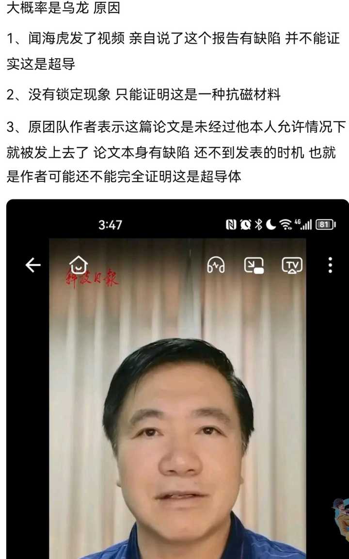
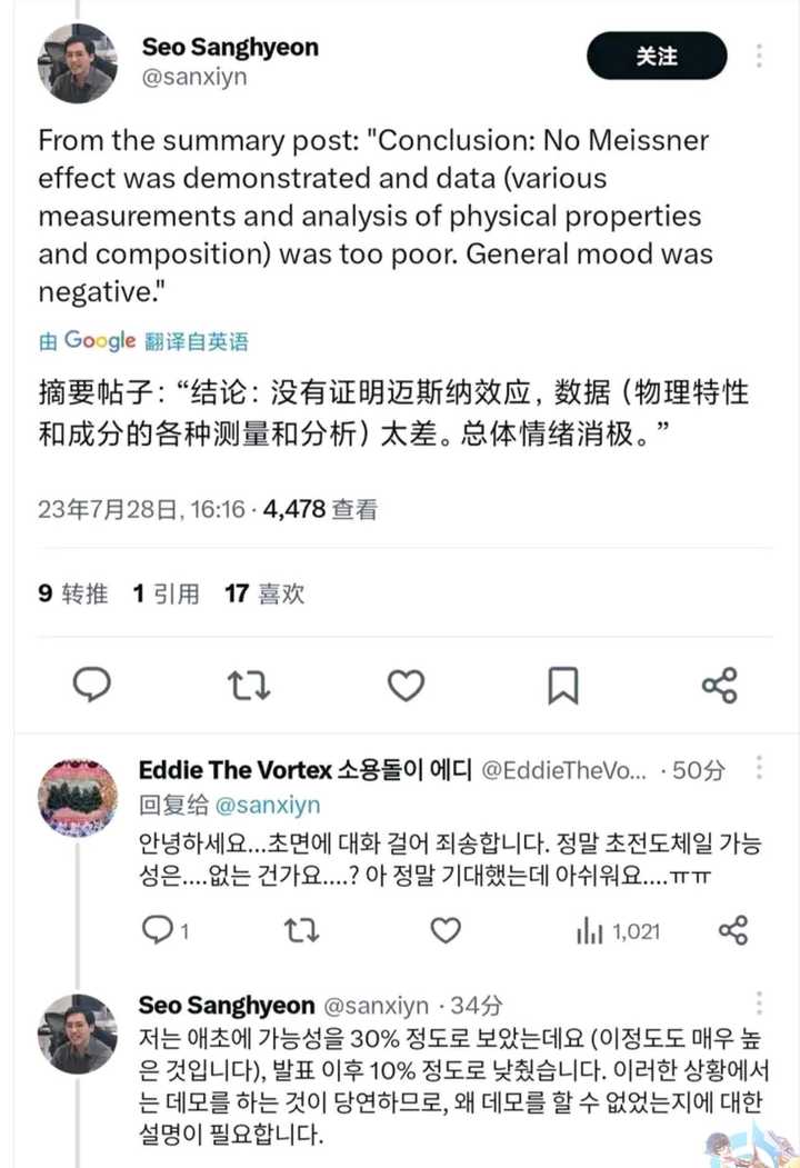
各大学纷纷在做复现实验,7月28日,南京大学物理学院教授闻海虎接受采访的表示:“我们仔细分析了他们的数据,从三个方面——电阻、磁化和所谓的磁悬浮,都不足以说明它是超导现象,我们判断极有可能是个假象。”

根据我搜查的各种消息,韩国那个团队确实是无意中发现了一个新的抗磁材料,但没有超导的锁定现象,按他论文里那个材料的性质,载流能力那么差,临街磁场那么低,实在难堪大用,离真正的室温超导八字没有一撇。

但这个消息太耸人听闻了,反而让人期待他是真的,咱们拭目以待吧,万一是真的,即使是韩国人取得的成就,也是造福全人类的,咱们不狭隘,每当人类文明遇到瓶颈,就需要这种石破天惊的突破来继续点亮下一步的科技树。
我们假设学界现在真的发现了如何研制超导材料并量产,对全人类有什么意义?能推动哪些产业进步,尤其是对咱们中国有哪些可能性?
第一,无论未来哪个国家科研团队发现了超导材料,都会发布在学界顶级的科研期刊上,这是全人类都可以享受的成果,基础理论层面的突破属于科学发现,不属于发明,不受专利权保护,没有任何国家可以据为己有。只要问世了,全世界谁都会去做复现实验,谁都可以去制造,谁也不可能独享。
第二,中国恰好是全世界工业制造业最发达的国家,而且是应用技术产业转化最快的国家之一,中国一定是会最早规模量产的,对我们完全是好事。
第三,超导材料就是0电阻的材料,特点就是电流0损耗,而且电流承载能力比普通材料强很多。这个东西一旦低成本大规模问世,毫无疑问将掀起巨大的产业革命,人类文明距离宇宙文明又更进一步。
如果需要用电的材料都替换为超导材料,那么用电效率极大提高,储存与传输的电能也极大提高,未来可能人人开上磁悬浮电动汽车,岂不是帅爆了。而且散热问题也得了极大的解决,各种需要用电的产品都会变的更加的轻薄。最重要的就是可控核聚变,核聚变产生极高的温度,没有任何常规材料可以包容,就需要超导材料产生的磁场约束,常温超导材料正好解决它民用量产的可能,那么人类的能源问题也就解决了,关键是就会有新时代的核聚变发动机问世,人类远征其它星球也就成为了可能,大宇宙时代将开启。
我是神灯,最天马行空的内容分享。
发布于 2023-07-29 20:19・IP 属地北京真诚赞赏,手留余香还没有人赞赏,快来当第一个赞赏的人吧!查看全文>>
神灯夜话 - 0 个点赞 👍
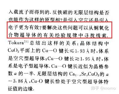
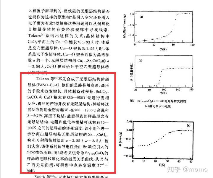
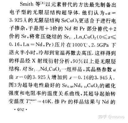
大佬我想请你看一下这个论文
这个论文是浙江大学物理系在1993的论文
其中这部分合成法和这次韩国团队的方法有关系吗?
我是纯外行,看不懂论文。
但这里提到了“铜氧化合物超导体”
类似的烧制过程
还有这个所谓的sr缺位引入的空穴和你的描述的晶格畸变好像有点关系
 编辑于 2023-07-29 23:54・IP 属地韩国
查看全文>>
momo